
How Photovoltaic Cells Work: Science & Innovation Explained
Category: Renewable Energy
Understanding How Photovoltaic Cells Work: From Basics to Innovation
Whether you're a curious beginner fascinated by solar energy or an electrical engineer looking to deepen your understanding of photovoltaic technology, this post is tailored for you. Today's growing demand for renewable energy sources means photovoltaic cells—or solar cells—are at the heart of converting sunlight into clean electricity. Yet, the science behind these cells can seem complex, filled with semiconductor physics, electron behavior, and material science. Many struggle with questions like how sunlight generates electric current, what role silicon plays, or how innovation is pushing efficiency boundaries further. You likely arrived here aiming to get a clear, step-by-step explanation that bridges fundamental principles with modern advancements in photovoltaic technology. This blog uniquely combines approachable explanations with in-depth insights, helping both novices grasp the essentials and engineers discover new perspectives. By focusing on the inner workings, material innovations, and practical applications, we'll unpack the photovoltaic effect, cell construction, performance factors, and emerging research areas in a structured way designed to enlighten and engage. Dive in to unravel the science that powers sustainable solar energy and fuels the future of renewable technologies.
- Understanding How Photovoltaic Cells Work: From Basics to Innovation
- The Photovoltaic Effect: The Science Behind Solar Cells
- Materials Used in Photovoltaic Cells
- Structure and Components of a Photovoltaic Cell
- How Photovoltaic Cells Generate Electricity: Step-by-Step Process
- Factors Affecting Photovoltaic Cell Efficiency
- Types of Photovoltaic Cells and Their Innovations
- Manufacturing Processes and Challenges
- Integration of Photovoltaic Cells into Solar Panels and Systems
- Emerging Innovations and Future Trends in Photovoltaics
- Applications and Real-World Impact of Photovoltaic Technology
The Photovoltaic Effect: The Science Behind Solar Cells
At the heart of every photovoltaic cell lies the photovoltaic effect, the fundamental physical process that converts sunlight into electricity. When sunlight—which is composed of tiny energy packets called photons—strikes a solar cell, these photons transfer their energy to electrons in the cell’s semiconductor material, typically silicon. This energy absorption excites the electrons, freeing them from their atomic bonds and creating electron-hole pairs—where the electron is negatively charged, and the hole it leaves behind acts as a positive charge carrier.
This generation of electron-hole pairs alone doesn't produce usable electric current. The key innovation lies in the internal electric field created by the p-n junction inside the solar cell. This built-in field drives the free electrons and holes in opposite directions, separating the charges and preventing them from recombining. By guiding electrons toward the n-type layer and holes toward the p-type layer, the cell establishes a flow of electrons when connected to an external circuit, thereby generating direct current (DC) electricity. The entire process can be summarized as:
- Absorption of photons with energy greater than the semiconductor bandgap.
- Generation of electron-hole pairs in the semiconductor.
- Separation of charge carriers by the internal electric field.
- Collection of electric current through external contacts.
Understanding the photovoltaic effect clarifies why material properties, surface engineering, and semiconductor design are critical to optimizing solar cell performance. Innovations that enhance photon absorption, increase charge carrier lifetimes, or improve the efficiency of charge separation directly impact the energy conversion efficiency of photovoltaic technology, driving forward the renewable energy revolution.

Image courtesy of Pixabay
Materials Used in Photovoltaic Cells
The semiconductor material at the core of a photovoltaic cell is crucial because it directly affects how efficiently sunlight is converted into electrical energy. The overwhelming industry standard is silicon, primarily due to its abundance, stability, and excellent semiconductor properties suitable for the photovoltaic effect. Silicon’s atomic structure creates an ideal bandgap (~1.1 eV) that balances efficient absorption of solar photons with minimal thermal losses, making it highly effective for solar energy conversion.
Silicon: The Semiconductor Backbone
Silicon used in photovoltaic cells comes in two main forms: crystalline silicon (c-Si) and amorphous silicon (a-Si). Crystalline silicon, often found as monocrystalline or polycrystalline wafers, offers high efficiency and durability, making it the preferred material for most commercial solar panels. Amorphous silicon, though less efficient, is used in thin-film solar technologies due to its flexibility and lower manufacturing costs.
Doping: Creating P-type and N-type Layers
To enable the creation of an internal electric field necessary for charge separation, pure silicon is doped with specific impurities, altering its electrical properties:
- N-type silicon: Doped with elements like phosphorus that have five valence electrons—one more than silicon. This extra electron becomes a free charge carrier, making n-type silicon rich in free electrons.
- P-type silicon: Doped with elements like boron, which have three valence electrons—one less than silicon. This creates “holes” or positive charge carriers.
When these two doped layers are joined, they form the critical p-n junction, establishing an internal electric field that drives the photovoltaic effect and directs electron flow.
Why Silicon Remains the Industry Standard
Despite emerging materials such as perovskites gaining attention for their promise of higher efficiencies and lower manufacturing costs, silicon remains dominant in the photovoltaic market because of:
- Abundance and affordability: Silicon is the second most abundant element in the Earth’s crust.
- Proven long-term stability: Silicon solar cells maintain performance over decades with minimal degradation.
- Established manufacturing infrastructure: Global supply chains and fabrication technologies are optimized for silicon-based cells.
- Balanced bandgap properties: Silicon’s bandgap is well-suited to the solar spectrum, maximizing photon absorption while limiting energy loss.
This combination of favorable electrical characteristics, economic factors, and technological maturity firmly secures silicon’s role as the foundational material in most photovoltaic systems worldwide. Understanding these material fundamentals sets the stage for exploring how innovations like multi-junction cells and novel materials aim to surpass silicon’s intrinsic efficiency limits in future solar technologies.

Image courtesy of Kindel Media
Structure and Components of a Photovoltaic Cell
To fully grasp how photovoltaic cells efficiently convert sunlight into electrical energy, it’s essential to understand their internal structure and key components. A typical photovoltaic cell is a multilayered semiconductor device designed to optimize light absorption, charge separation, and current collection. Below is a breakdown of the main layers and components that make modern solar cells function effectively.
The P-N Junction: Heart of Charge Separation
At the core of every photovoltaic cell lies the p-n junction, where the p-type and n-type silicon layers meet. This junction forms an internal electric field critical for the photovoltaic effect:
- P-type layer: Doped with elements like boron, rich in positive charge carriers (holes).
- N-type layer: Doped with phosphorus, rich in free electrons.
The p-n junction creates a depletion region devoid of free charge carriers, establishing a built-in electric field. When sunlight generates electron-hole pairs near this region, the field swiftly separates and directs electrons toward the n-side and holes toward the p-side. This directional charge movement prevents recombination and initiates a steady flow of electric current when the cell is connected to an external load.
Anti-Reflective Coating: Maximizing Photon Absorption
Silicon surfaces naturally reflect a significant portion of incident sunlight—sometimes up to 30%. To reduce these reflection losses, a thin anti-reflective coating (ARC) is applied on top of the cell. This coating, typically made of silicon nitride or titanium dioxide, serves several vital functions:
- Reduces reflectance: Allows more photons to enter the cell, increasing light absorption.
- Protects the silicon surface: Shields the semiconductor from environmental damage and contamination.
- Enhances cell efficiency: By boosting photon capture, the ARC contributes directly to improved electrical output.
Electrodes: Conducting the Generated Current
Efficient charge collection is crucial to maintain the flow of electricity generated within the cell. Photovoltaic cells feature two types of electrodes:
- Front contact (usually a fine grid): Made from conductive metals such as silver or aluminum, this grid covers the cell surface but is designed to minimize shading, balancing transparency with conductivity.
- Rear contact (solid metal layer): Serves as a reflector to bounce unabsorbed light back into the cell and collects electrons to complete the electrical circuit.
These electrodes connect the cell to external circuits, enabling generated electrons to flow as usable direct current (DC) electricity.
Summary of Core Photovoltaic Cell Components
| Component | Function |
|---|---|
| P-N Junction | Creates internal electric field to separate and direct charge carriers |
| Anti-Reflective Coating | Minimizes sunlight reflection, enhances photon absorption |
| Front Electrode | Collects electrons, designed to reduce light shading with fine metal grid |
| Rear Electrode | Collects electrons and reflects light back into the cell for improved absorption |
Understanding the structure and components of photovoltaic cells reveals how precise engineering at the micro-level enables efficient solar energy conversion. These layers work synergistically to capture sunlight, separate charges rapidly, and deliver electrical power reliably—forming the foundation upon which innovations in solar technology continue to build.
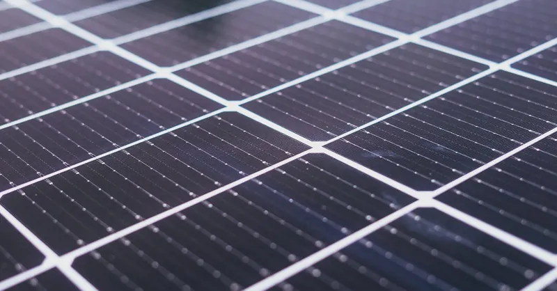
Image courtesy of Los Muertos Crew
How Photovoltaic Cells Generate Electricity: Step-by-Step Process
The conversion of sunlight into usable electrical energy within a photovoltaic (PV) cell involves a precise series of physical and electrical phenomena working seamlessly together. Understanding this step-by-step process is essential to appreciate the sophistication behind solar power generation and to identify opportunities for efficiency improvements.
-
Photon Absorption: When sunlight reaches the photovoltaic cell, photons with energy equal to or greater than the semiconductor’s bandgap penetrate the anti-reflective coating and enter the silicon layers. These photons excite electrons by transferring their energy, which is the fundamental trigger that initiates electricity generation.
-
Generation of Electron-Hole Pairs: The absorbed photon energy frees electrons from the silicon atoms, creating mobile electrons (negative charge carriers) and corresponding holes (positive charge carriers). This process is called electron-hole pair generation and primarily occurs within or near the depletion region of the p-n junction where the internal electric field is strongest.
-
Charge Carrier Separation: The built-in electric field across the p-n junction acts as a directional force that pushes electrons toward the n-type layer and holes toward the p-type layer. This separation prevents immediate recombination, ensuring that the charge carriers remain free to move and contribute to electric current.
-
Charge Collection and Flow through External Circuit: Once separated, electrons are collected by the front electrode (usually a fine metal grid) and flow through an external load before returning via the rear electrode to the p-type side. This movement of electrons through the external circuit constitutes a direct current (DC), which can be harnessed to power electrical devices.
-
Recombination Minimization: Throughout this process, minimizing the recombination of electrons and holes—where they annihilate each other without generating current—is vital. High-quality materials, surface passivation, and optimized cell design reduce recombination losses, enhancing overall cell efficiency.
This stepwise transformation highlights why factors like semiconductor purity, doping precision, and surface treatments critically influence photovoltaic cell performance. Innovations such as multi-layer anti-reflective coatings, passivated emitter and rear cell (PERC) technology, and textured surfaces are engineered explicitly to maximize photon absorption, improve charge carrier lifetimes, and optimize current extraction, pushing solar cell efficiencies to new heights.
By mastering this detailed sequence of physical events, engineers and enthusiasts alike can better understand how sunlight—one of the most abundant renewable resources—is effectively converted into clean, sustainable electricity that powers homes, businesses, and the broader energy grid worldwide.

Image courtesy of Kindel Media
Factors Affecting Photovoltaic Cell Efficiency
Maximizing the energy conversion efficiency of photovoltaic cells is a critical goal in solar technology development. Understanding the main factors that influence efficiency not only helps in optimizing current systems but also drives innovation for next-generation solar cells. Several intrinsic and environmental aspects can significantly impact how effectively a photovoltaic cell converts sunlight into usable electricity.
Internal Recombination Losses
One of the primary internal efficiency barriers in photovoltaic cells is recombination, the process where free electrons and holes annihilate each other before contributing to the electric current. Recombination can occur within the bulk semiconductor material or at surfaces and interfaces, reducing the number of charge carriers available for current generation. Key types include:
- Bulk recombination: Caused by impurities or defects within the silicon crystal lattice that trap carriers.
- Surface recombination: Occurs where the silicon meets other materials or air, where dangling bonds and imperfections increase recombination risk.
- Auger recombination: An intrinsic effect predominant at high carrier concentrations, where energy is transferred to another electron instead of producing current.
Reducing recombination through high-purity silicon, surface passivation techniques, and optimized cell architecture is essential for improving efficiency.
Light Absorption and Spectral Response
Efficient light absorption is fundamental to generating a high number of electron-hole pairs. Factors influencing absorption include:
- Material bandgap: Determines which photon energies can be absorbed; silicon’s bandgap (~1.1 eV) captures a broad range of the solar spectrum but misses some high and low-energy photons.
- Surface texture and anti-reflective coatings: Enhance photon capture by reducing reflection and increasing the effective optical path within the cell.
- Thickness of the semiconductor layer: Thicker layers absorb more light but can increase recombination; balancing this is essential.
Advanced designs such as tandem or multi-junction cells layer different materials with varying bandgaps to capture more spectral energy, pushing beyond single-junction efficiency limits.
Temperature Effects
Photovoltaic cells are sensitive to temperature variations, which notably affect their electrical characteristics:
- Higher temperatures generally reduce the open-circuit voltage (Voc) due to increased intrinsic carrier generation, negatively impacting the cell’s power output.
- Excess heat can accelerate material degradation and reduce long-term reliability.
- Optimal operating conditions typically range between 25°C (standard test condition) and moderately elevated temperatures; above this, efficiency drops.
Effective thermal management through module design, ventilation, or heat dissipation techniques is vital, especially in hot climates, to maintain peak performance.
Impact of Shading and Partial Illumination
Shading—even partial coverage of a photovoltaic cell or panel area—can drastically reduce overall power output because it interrupts the uniform current flow within solar modules. Consequences include:
- Reduced energy generation and localized heating known as hot spots that can damage cells.
- Bypass diodes and module-level power electronics such as microinverters or power optimizers are used to mitigate shading effects and maintain performance.
Site planning to minimize shading and the use of intelligent module design ensure more consistent energy harvest under varying environmental conditions.
By addressing these key factors—internal recombination, light absorption, temperature, and shading—engineers can strategically enhance photovoltaic cell efficiency, underpinning the continual push towards more cost-effective and powerful solar energy solutions.

Image courtesy of Kindel Media
Types of Photovoltaic Cells and Their Innovations
Photovoltaic technology encompasses a variety of cell types, each designed with unique materials and structures to optimize solar energy conversion under different conditions. Understanding the distinctions between monocrystalline, polycrystalline, and thin-film cells, as well as emerging technologies like perovskite and multi-junction cells, is crucial for grasping how innovation drives efficiency and adaptability in solar power systems.
Monocrystalline Photovoltaic Cells
Monocrystalline cells are made from single-crystal silicon wafers, produced through a highly controlled crystal growth process. This uniform crystalline structure allows for:
- High efficiency rates (typically 20% and above) due to superior electron mobility and minimal defects.
- Long-term durability and stability, making them ideal for residential and commercial solar installations where footprint and performance are priorities.
- A sleek black appearance, preferred aesthetically in many solar panel designs.
However, monocrystalline cells require more energy-intensive manufacturing and have higher production costs compared to other cell types.
Polycrystalline Photovoltaic Cells
Polycrystalline cells, also called multicrystalline, consist of multiple small silicon crystals melted together to form the wafer. Key characteristics include:
- Lower manufacturing costs owing to simpler production methods.
- Slightly lower efficiency (typically 15–17%) compared to monocrystalline cells due to grain boundaries that impede electron flow.
- A distinctive blue-speckled appearance caused by the multiple crystal grains.
Polycrystalline cells strike a balance between cost and efficiency, making them popular for large-scale solar farms where maximizing area is more important than peak efficiency.
Thin-Film Photovoltaic Cells
Thin-film technologies use very thin layers of semiconductor materials deposited on substrates like glass, plastic, or metal. Popular thin-film types include:
- Amorphous silicon (a-Si): Flexible but lower efficiency (~6–9%), used in niche applications like building-integrated photovoltaics.
- Cadmium telluride (CdTe) and Copper indium gallium selenide (CIGS): Offer higher efficiencies (~11–15%) with potentially lower manufacturing costs and better performance in low-light conditions.
Thin-film cells excel in flexibility, lightweight design, and cost-effectiveness, but generally exhibit lower efficiencies and shorter lifespans compared to crystalline silicon cells.
Emerging Technologies: Perovskites and Multi-Junction Cells
Cutting-edge research is pushing the boundaries of photovoltaic performance with novel materials and designs:
- Perovskite Solar Cells:
- Utilize a class of crystal structures known as perovskites that have demonstrated rapid efficiency improvements, reaching over 25% in laboratory settings.
- Offer potential for low-cost, solution-based manufacturing processes, and the ability to be integrated atop silicon cells in tandem configurations.
-
Challenges remain around long-term stability and scalability, but perovskites are a front-runner for next-generation solar technologies.
-
Multi-Junction Solar Cells:
- Comprise stacked layers of semiconductors with different bandgaps, allowing them to capture a broader range of the solar spectrum.
- Achieve record-breaking efficiencies exceeding 40% in concentrator photovoltaic (CPV) applications.
- Typically used in specialized fields such as space solar power and high-efficiency concentrator systems due to their complex manufacturing and cost.
By leveraging these diverse photovoltaic cell types and innovations, solar technology continues to evolve — improving efficiency, lowering costs, and expanding the potential applications of clean, renewable energy worldwide. Whether you prioritize durability, cost-effectiveness, or cutting-edge performance, understanding these options is key to selecting and developing the optimal photovoltaic solutions for future energy needs.
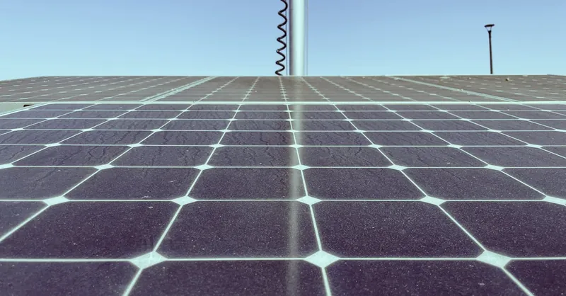
Image courtesy of Kindel Media
Manufacturing Processes and Challenges
The production of high-quality photovoltaic (PV) cells involves complex manufacturing processes that directly influence the efficiency, durability, and cost of solar technology. Central to these processes is the fabrication of silicon wafers, precise doping procedures to create effective p-n junctions, and the meticulous layering of multiple materials for optimized light absorption and charge collection. Each step must balance performance goals with scalability and economic feasibility in an increasingly competitive renewable energy market.
Wafer Production: From Silicon to Solar-Ready Substrate
The foundation of most PV cells is the silicon wafer, which begins as ultra-pure silicon produced through the Czochralski or float-zone methods to form single-crystal or multicrystalline ingots. These ingots are then sliced into extremely thin wafers—typically around 150-200 micrometers thick—ensuring minimal material waste and precise thickness uniformity to optimize light absorption and mechanical stability.
Key challenges in wafer production include:
- Reducing silicon waste during slicing, as kerf loss can account for a significant portion of raw material loss.
- Ensuring crystal uniformity and low defect density to minimize recombination centers that degrade cell efficiency.
- Scaling up production capacity without compromising wafer quality or dramatically increasing costs.
Advances like diamond wire sawing and thinner wafers are helping to address these challenges by improving cutting efficiency and material utilization.
Doping and Layering: Engineering Electrical Properties
After wafer preparation, doping introduces controlled impurities—such as phosphorus for n-type and boron for p-type layers—that establish the critical internal electric field at the p-n junction. This doping must be precise, uniform, and stable to maintain consistent cell performance. Methods like diffusion doping and ion implantation are widely used, each with trade-offs in complexity, cost, and doping depth control.
Following doping, sophisticated layering processes apply:
- Anti-reflective coatings (ARCs) to reduce photon reflection and enhance light capture.
- Passivation layers that protect cell surfaces and minimize recombination at interfaces.
- Metallic contacts, deposited via screen printing or evaporation, forming the front and rear electrodes necessary for efficient current collection.
Innovations such as passivated emitter and rear cell (PERC) designs incorporate additional layers to reflect unabsorbed light and passivate rear surfaces, significantly boosting efficiency.
Cost-Related Manufacturing Challenges
While silicon remains abundant, the cost of PV cell manufacturing is a pivotal factor driving solar adoption. Balancing high performance with affordable production demands addressing several challenges:
- Material Costs: High-purity silicon and specialty gases used in doping and coating processes contribute significantly to overall expenses.
- Energy-Intensive Processes: Crystal growth, wafer slicing, and high-temperature treatments consume considerable energy, impacting both cost and environmental footprint.
- Equipment and Process Complexity: Advanced manufacturing techniques require substantial capital investment and sophisticated quality control to maintain yield and consistency.
- Scaling Production: Meeting global demand calls for rapid expansion of manufacturing facilities without sacrificing process refinement or product reliability.
Ongoing research is focused on reducing costs through thin wafer production, innovative doping techniques, and automation to streamline manufacturing workflows. Additionally, emerging materials and cell architectures seek to simplify fabrication steps while preserving or enhancing efficiency—paving the way for more accessible and widespread solar technology deployment.
Understanding the intricate balance between manufacturing precision and cost-efficiency is essential for engineers and industry stakeholders aiming to drive the photovoltaic sector toward a sustainable, economically viable future.
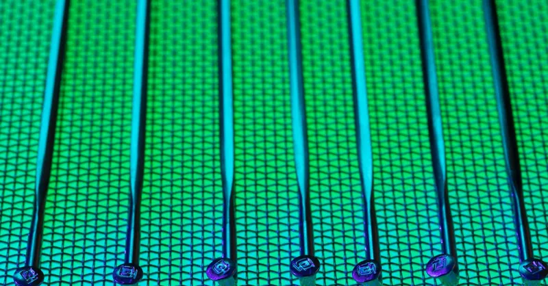
Image courtesy of Nic Wood
Integration of Photovoltaic Cells into Solar Panels and Systems
Photovoltaic (PV) cells are the fundamental units for converting sunlight into electricity, but to generate usable power at scale, individual cells must be precisely integrated into larger solar panels and systems. This integration involves electrically connecting cells in series and parallel configurations, assembling them into durable modules, and carefully designing the overall system to optimize performance, reliability, and scalability.
Series and Parallel Connections: Balancing Voltage and Current
Individual solar cells typically produce a low voltage (around 0.5–0.6 volts) but can generate significant current. To achieve the voltage and current levels required by various applications, cells are combined through:
- Series Connections:
- Cells connected end-to-end increase the total voltage of the string, adding each cell’s voltage while maintaining the same current.
- For example, connecting 36 cells in series produces approximately 18 V DC, suitable for common residential panels.
-
Series wiring is vital for reaching inverter input voltage requirements and minimizing losses over cable runs.
-
Parallel Connections:
- Multiple series strings can be connected in parallel to increase the current capacity while maintaining the same voltage output.
- Parallel wiring enhances total power output and provides redundancy; if one string is shaded or faulty, others can continue operating.
- Careful design is needed to ensure current sharing and to avoid mismatches that reduce system efficiency.
The combination of series and parallel architectures allows flexible tailoring of solar panels and arrays to match the desired power specifications and electrical system constraints.
Panel Assembly: From Cells to Modules
After electrical interconnection, cells are encapsulated and assembled into complete solar panels through several critical steps:
- Encapsulation: Cells are sandwiched between protective layers such as tempered glass on the front and durable polymer back sheets. This protects against moisture, UV exposure, and mechanical damage.
- Framing and Sealing: Aluminum frames provide structural integrity and facilitate mounting, while sealing materials prevent environmental ingress.
- Junction Boxes and Bypass Diodes: Junction boxes house electrical contacts and include bypass diodes that protect against hotspot formation and power loss when part of the panel is shaded or damaged.
These assembly practices ensure long-term durability, weather resistance, and consistent electrical performance, enabling panels to operate efficiently in diverse environmental conditions for decades.
System Design Considerations
Integrating photovoltaic modules into complete solar power systems requires attention to several design factors:
- Matching Electrical Characteristics: Panels must be selected or configured to match the inverter input voltage and current ratings for optimal energy conversion.
- Shade Management: Since shading on even a small portion of cells can disproportionately affect panel output, system layouts minimize shading and incorporate bypass diodes or module-level power electronics to mitigate losses.
- Thermal Management: Panel placement and system ventilation must address heat dissipation to prevent efficiency drops due to high operating temperatures.
- Wiring and Protection: Proper wiring gauges, conduit protection, and electrical safety components (e.g., fuses, disconnects) are essential for reliability and compliance with electrical codes.
- Scalability and Maintenance: Modular panel design and string configurations facilitate system expansion, ease diagnostics, and simplify maintenance routines.
Understanding how photovoltaic cells are interconnected and packaged into sophisticated systems provides critical insight into the practical deployment of solar energy solutions. The synergy of electrical and mechanical design enables solar panels to convert individual cell currents into robust, high-voltage DC power streams ready for grid integration or standalone use—empowering the global clean energy transition.

Image courtesy of Markus Spiske
Emerging Innovations and Future Trends in Photovoltaics
As the demand for clean and affordable energy soars, photovoltaic (PV) technology continues to evolve rapidly through groundbreaking innovations aimed at boosting efficiency and reducing costs. Moving beyond traditional silicon cells, researchers and engineers are developing novel materials and architectures that promise to transform solar energy harvesting and expand its applications.
Tandem and Multi-Junction Solar Cells
One of the most significant advancements in PV technology is the emergence of tandem solar cells, which stack multiple semiconductor layers with different bandgaps to capture a broader range of the solar spectrum. By combining materials such as silicon with perovskites or other semiconductors, tandem cells can:
- Increase overall energy conversion efficiency well beyond silicon’s single-junction Shockley-Queisser limit (around 29%).
- Reduce thermal losses by optimizing photon absorption across high-energy and low-energy wavelengths.
- Open pathways for commercial deployment in rooftop, utility-scale, and even flexible solar modules.
State-of-the-art multi-junction cells have demonstrated laboratory efficiencies exceeding 40%, representing a substantial leap forward in photovoltaic performance, particularly for specialized applications like space and concentrator photovoltaics (CPV).
Flexible and Lightweight Photovoltaic Technologies
Traditional silicon solar panels, while efficient, are inherently rigid and comparatively heavy, limiting their installation versatility. In contrast, flexible photovoltaics based on thin films or organic materials are gaining traction due to their:
- Bendable, lightweight nature, enabling integration into curved surfaces, portable electronics, and building-integrated photovoltaics (BIPV).
- Potential for roll-to-roll manufacturing, which can dramatically reduce production costs and increase scalability.
- Suitability for novel applications such as solar-powered wearables, vehicles, and infrastructure where traditional panels are impractical.
Emerging flexible PV materials—including perovskites, organic photovoltaics (OPVs), and CIGS thin films—are steadily improving their durability and efficiency, narrowing the gap with crystalline silicon modules.
Enhanced Materials and Surface Engineering
Material science innovations continue to refine photovoltaic performance by focusing on enhanced light management and charge carrier dynamics:
- Perovskite materials exhibit exceptional tunability in bandgaps and strong light absorption, enabling versatile designs from standalone cells to tandem layers atop silicon.
- Advanced surface passivation techniques reduce recombination losses by minimizing defects and dangling bonds at semiconductor interfaces.
- Nanostructured coatings and light-trapping architectures, such as textured surfaces or photonic crystals, increase the optical path length within solar cells, maximizing photon absorption even in thinner layers.
- Experimentation with emerging semiconductors like kesterites and environmentally friendly materials aims to balance efficiency with sustainability and cost.
These materials and engineering breakthroughs are instrumental in pushing photovoltaic cells towards higher efficiency thresholds while maintaining or lowering manufacturing costs.
Digitalization and Smart PV Systems
Future photovoltaic systems are increasingly integrating digital technologies such as artificial intelligence (AI), machine learning, and advanced sensor networks to optimize energy harvest and system reliability. Smart tracking, predictive maintenance, and adaptive control algorithms enable:
- Real-time performance optimization adjusted for shading, soiling, and weather variability.
- Enhanced lifespan prediction and fault detection for reducing operational costs.
- Integration with energy storage and grid management systems to support steady renewable power supply.
This convergence of photovoltaic innovation with digital intelligence marks a critical step toward fully autonomous, efficient, and cost-effective solar energy solutions.
By harnessing tandem architectures, flexible materials, advanced surface engineering, and smart system designs, the future of photovoltaics is poised to deliver unprecedented efficiency gains, lower costs, and broader adoption—accelerating the global transition to clean and sustainable energy.
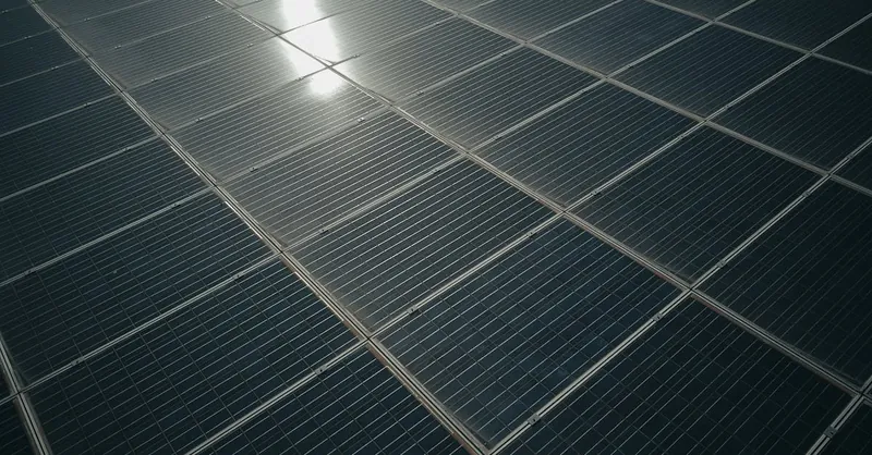
Image courtesy of Kindel Media
Applications and Real-World Impact of Photovoltaic Technology
Photovoltaic (PV) technology has become a cornerstone of the global renewable energy landscape, powering a diverse range of applications from small residential rooftops to massive utility-scale solar farms. Its versatility and scalability make it a preferred choice for clean electricity generation across different sectors. Understanding these practical implementations illustrates not only the technological maturity of solar power but also its profound impact on energy sustainability and carbon footprint reduction.
Residential and Commercial Rooftop Solar Systems
One of the most widespread applications of photovoltaic cells is in residential rooftop solar panels, which enable homeowners to generate their own electricity, reduce energy bills, and contribute to grid decarbonization. These systems typically feature:
- Modular solar panels installed on south-facing roofs for optimum sunlight exposure.
- Integration with inverters to convert DC electricity into AC usable by household appliances.
- Optional battery storage units that store excess energy for nighttime use or grid outages.
- Smart energy management systems allowing users to monitor production and consumption in real-time.
Residential solar fosters energy independence, lowers greenhouse gas emissions, and increases property value, making it a key driver in the democratization of solar energy.
Similarly, commercial rooftop arrays serve businesses by providing significant electricity cost savings, enhancing corporate sustainability profiles, and fulfilling renewable energy mandates. The larger scale and higher energy demands in commercial settings enable the use of more powerful inverter systems and often incorporate net metering policies, allowing excess electricity to be fed back into the grid for credit.
Utility-Scale Solar Farms
At the other end of the spectrum, large-scale solar farms harness vast photovoltaic arrays to generate electricity for thousands of homes and businesses. These farms:
- Utilize hundreds to thousands of solar panels arranged in optimized layouts to maximize sunlight capture over large land areas.
- Incorporate advanced tracking systems that tilt panels to follow the sun, increasing total energy yield.
- Connect directly to regional or national power grids, contributing substantial renewable energy capacity.
- Often pair with energy storage systems or complementary renewable installations like wind farms to balance supply and demand.
Solar farms contribute significantly to national renewable energy targets and help reduce reliance on fossil fuel power plants, aiding in combating climate change on a broad scale.
Off-Grid and Remote Power Applications
Photovoltaic cells are also crucial in providing electricity to off-grid locations such as remote villages, islands, or scientific research stations where conventional grid access is impractical or costly. In these scenarios, PV systems:
- Are combined with battery banks and charge controllers to store and regulate power for continuous use.
- Enable telecommunications infrastructure, water pumping, and lighting, improving quality of life and economic opportunities.
- Serve as a reliable, low-maintenance alternative to diesel generators, reducing greenhouse gas emissions and operational costs.
The expansion of off-grid solar solutions exemplifies the social and environmental benefits of photovoltaic technology, delivering sustainable energy access to under-served populations globally.
By powering everything from individual homes to large power grids and remote communities, photovoltaic technology proves its indispensable role in the transition toward a cleaner, more resilient energy future. Its ability to scale, integrate, and adapt across various real-world applications ensures that solar energy continues to be a driving force in global renewable energy deployment.
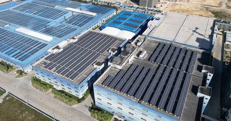
Image courtesy of Nova lv